
Saturday, 30 September 2017
Friday, 29 September 2017
Voltage drop
Voltage drop describes how energy is supplied of a voltage source that is reduced as electric current moves through the passive elements (elements that do not supply voltage) of an electrical circuit. Voltage drops across internal resistances of the source, across conductors, across contacts, and across connectors are undesired as the supplied energy is lost (dissipated). Voltage drops across loads and across other active circuit elements are desired as the supplied energy performs useful work.
For example, an electric space heater may have a resistance of ten ohms, and the wires which supply it may have a resistance of 0.2 ohms, about 2% of the total circuit resistance. This means that approximately 2% of the supplied voltage is lost in the wire itself. Excessive voltage drop may result in unsatisfactory operation of, and damage to, electrical and electronic equipment.
National and local electrical codes may set guidelines for the maximum voltage drop allowed in electrical wiring, to ensure efficiency of distribution and proper operation of electrical equipment. The maximum permitted voltage drop varies from one country to another.n electronic design and power transmission, various techniques are employed to compensate for the effect of voltage drop on long circuits or where voltage levels must be accurately maintained. The simplest way to reduce voltage drop is to increase the diameter of the conductor between the source and the load, which lowers the overall resistance. In power distribution systems, a given amount of power can be transmitted with less voltage drop if a higher voltage is used. More sophisticated techniques use active elements to compensate for the undesired voltage drop.
If the voltage between the DC source and the first resistor (67 ohms) is measured, the voltage potential at the first resistor will be slightly less than nine volts. The current passes through the conductor (wire) from the DC source to the first resistor; as this occurs, some of the supplied energy is "lost" (unavailable to the load), due to the resistance of the conductor. Voltage drop exists in both the supply and return wires of a circuit. If the voltage across each resistor is measured, the measurement will be a significant number. That represents the energy used by the resistor. The larger the resistor, the more energy used by that resistor, and the bigger the voltage drop across that resistor.
Ohm's Law can be used to verify voltage drop. In a DC circuit, voltage equals current multiplied by resistance. . Also, Kirchhoff's circuit laws state that in any DC circuit, the sum of the voltage drops across each component of the circuit is equal to the supply voltage.
Electrical impedance is commonly represented by the variable Z and measured in ohms at a specific frequency. Electrical impedance is computed as the vector sum of electrical resistance, capacitive reactance, and inductive reactance.
The amount of impedance in an alternating-current circuit depends on the frequency of the alternating current and the magnetic permeability of electrical conductors and electrically isolated elements (including surrounding elements), which varies with their size and spacing.
Analogous to Ohm's law for direct-current circuits, electrical impedance may be expressed by the formula . So, the voltage drop in an AC circuit is the product of the current and the impedance of the circuit.
For example, an electric space heater may have a resistance of ten ohms, and the wires which supply it may have a resistance of 0.2 ohms, about 2% of the total circuit resistance. This means that approximately 2% of the supplied voltage is lost in the wire itself. Excessive voltage drop may result in unsatisfactory operation of, and damage to, electrical and electronic equipment.
National and local electrical codes may set guidelines for the maximum voltage drop allowed in electrical wiring, to ensure efficiency of distribution and proper operation of electrical equipment. The maximum permitted voltage drop varies from one country to another.n electronic design and power transmission, various techniques are employed to compensate for the effect of voltage drop on long circuits or where voltage levels must be accurately maintained. The simplest way to reduce voltage drop is to increase the diameter of the conductor between the source and the load, which lowers the overall resistance. In power distribution systems, a given amount of power can be transmitted with less voltage drop if a higher voltage is used. More sophisticated techniques use active elements to compensate for the undesired voltage drop.
Voltage drop in direct-current circuits: resistance
Consider a direct-current circuit with a nine-volt DC source; three resistors of 67 ohms, 100 ohms, and 470 ohms; and a light bulb—all connected in series. The DC source, the conductors (wires), the resistors, and the light bulb (the load) all have resistance; all use and dissipate supplied energy to some degree. Their physical characteristics determine how much energy. For example, the DC resistance of a conductor depends upon the conductor's length, cross-sectional area, type of material, and temperature.If the voltage between the DC source and the first resistor (67 ohms) is measured, the voltage potential at the first resistor will be slightly less than nine volts. The current passes through the conductor (wire) from the DC source to the first resistor; as this occurs, some of the supplied energy is "lost" (unavailable to the load), due to the resistance of the conductor. Voltage drop exists in both the supply and return wires of a circuit. If the voltage across each resistor is measured, the measurement will be a significant number. That represents the energy used by the resistor. The larger the resistor, the more energy used by that resistor, and the bigger the voltage drop across that resistor.
Ohm's Law can be used to verify voltage drop. In a DC circuit, voltage equals current multiplied by resistance. . Also, Kirchhoff's circuit laws state that in any DC circuit, the sum of the voltage drops across each component of the circuit is equal to the supply voltage.

Voltage drop in alternating-current circuits: impedance
In alternating-current circuits, opposition to current flow occurs because of resistance, just as in direct-current circuits. However, alternating current circuits also include a second kind of opposition to current flow: reactance. The sum of oppositions to current flow from both resistance and reactance is called impedance.Electrical impedance is commonly represented by the variable Z and measured in ohms at a specific frequency. Electrical impedance is computed as the vector sum of electrical resistance, capacitive reactance, and inductive reactance.
The amount of impedance in an alternating-current circuit depends on the frequency of the alternating current and the magnetic permeability of electrical conductors and electrically isolated elements (including surrounding elements), which varies with their size and spacing.
Analogous to Ohm's law for direct-current circuits, electrical impedance may be expressed by the formula . So, the voltage drop in an AC circuit is the product of the current and the impedance of the circuit.

Thursday, 28 September 2017
PC test bench Plans
hi and welcome to a quick post showing off my pc test bench plans that I am planning to build in an upcoming project day the main uses for this will be testing different hardware configurations without putting them into case this is only a basic drawing with a lot more details in the build post
 the main parts of this project is the motherboard mounting which is on the top of the bench which will have different mounting holes for different types of boards as wellas a hard drive mounting board that will include some usb ports and testing leds
dobby

dobby
Wednesday, 27 September 2017
Low-frequency oscillation
Low-frequency oscillation (LFO) is an electronic signal which is usually below 20 Hz and creates a rhythmic pulse or sweep. This pulse or sweep is often used to modulate synthesizers, delay lines and other audio equipment in order to create effects used in the production of electronic music. Audio effects such as vibrato, tremolo and phasing are examples. The abbreviation LFO is also very often used to refer to low-frequency oscillators themselves.
Using a low-frequency oscillation signal as a means of modulating another signal introduces complexities into the resulting sound, such that a variety of effects can be achieved. The specifics vary greatly depending on the type of modulation, the relative frequencies of the LFO signal and the signal being modulated, et cetera.
History
Low-frequency oscillation as a concept was first introduced in the modular synths of the 1960s and 70s. Often the LFO effect was accidental, so there were myriad configurations that could be 'patched' by the synth operator. LFOs have since appeared in some form on almost every synthesizer. More recently other electronic musical instruments, such as samplers and software synthesizers, have included LFOs to increase their sound alteration capabilities.Overview
The primary oscillator circuits of a synthesizer are used to create the audio signals. A LFO is a secondary oscillator that operates at a significantly lower frequency (hence its name), typically below 20 Hz. This lower frequency or control signal is used to modulate another component's value, changing the sound without introducing another source. Like a standard oscillator, this usually takes the form of a periodic waveform, such as a sine, sawtooth, triangle or square wave. Also like a standard oscillator, LFOs can incorporate any number of waveform types, including user-defined wavetables, rectified waves and random signals.Using a low-frequency oscillation signal as a means of modulating another signal introduces complexities into the resulting sound, such that a variety of effects can be achieved. The specifics vary greatly depending on the type of modulation, the relative frequencies of the LFO signal and the signal being modulated, et cetera.
Tuesday, 26 September 2017
Breadboards
A breadboard is a construction base for prototyping of electronics. Originally it was literally a bread board, a polished piece of wood used for slicing bread. In the 1970s the solderless breadboard (AKA plugboard, a terminal array board) became available and nowadays the term "breadboard" is commonly used to refer to these.
Because the solderless breadboard does not require soldering, it is reusable. This makes it easy to use for creating temporary prototypes and experimenting with circuit design. For this reason, solderless breadboards are also extremely popular with students and in technological education. Older breadboard types did not have this property. A stripboard (Veroboard) and similar prototyping printed circuit boards, which are used to build semi-permanent soldered prototypes or one-offs, cannot easily be reused. A variety of electronic systems may be prototyped by using breadboards, from small analog and digital circuits to complete central processing units (CPUs).
Breadboards have evolved over time, with the term now being used for all kinds of prototype electronic devices. For example, US Patent 3,145,483,was filed in 1961 and describes a wooden plate breadboard with mounted springs and other facilities. US Patent 3,496,419,was filed in 1967 and refers to a particular printed circuit board layout as a Printed Circuit Breadboard. Both examples refer to and describe other types of breadboards as prior art.
The breadboard most commonly used today is usually made of white plastic and is a pluggable (solderless) breadboard. It was designed by Ronald J. Portugal in 1971.
Modern circuit designs are generally developed using a schematic capture and simulation system, and tested in software simulation before the first prototype circuits are built on a printed circuit board. Integrated circuit designs are a more extreme version of the same process: since producing prototype silicon is costly, extensive software simulations are performed before fabricating the first prototypes. However, prototyping techniques are still used for some applications such as RF circuits, or where software models of components are inexact or incomplete.
You could also use a square grid of pairs of holes where one hole per pair connects to its row and the other connects to its column. This same shape can be in a circle with rows and columns each spiraling opposite clockwise/counterclockwise.
The spacing between the clips (lead pitch) is typically 0.1 in (2.54 mm). Integrated circuits (ICs) in dual in-line packages (DIPs) can be inserted to straddle the centerline of the block. Interconnecting wires and the leads of discrete components (such as capacitors, resistors, and inductors) can be inserted into the remaining free holes to complete the circuit. Where ICs are not used, discrete components and connecting wires may use any of the holes. Typically the spring clips are rated for 1 ampere at 5 volts and 0.333 amperes at 15 volts (5 watts). The edge of the board has male and female notches so boards can be clipped together to form a large breadboard.
In a more robust variant, one or more breadboard strips are mounted on a sheet of metal. Typically, that backing sheet also holds a number of binding posts. These posts provide a clean way to connect an external power supply. This type of breadboard may be slightly easier to handle. Several images in this article show such solderless breadboards.
Differently colored wires and color-coding discipline are often adhered to for consistency. However, the number of available colors is typically far fewer than the number of signal types or paths. Typically, a few wire colors are reserved for the supply voltages and ground (e.g., red, blue, black), some are reserved for main signals, and the rest are simply used where convenient. Some ready-to-use jump wire sets use the color to indicate the length of the wires, but these sets do not allow a meaningful color-coding schema.
Because the solderless breadboard does not require soldering, it is reusable. This makes it easy to use for creating temporary prototypes and experimenting with circuit design. For this reason, solderless breadboards are also extremely popular with students and in technological education. Older breadboard types did not have this property. A stripboard (Veroboard) and similar prototyping printed circuit boards, which are used to build semi-permanent soldered prototypes or one-offs, cannot easily be reused. A variety of electronic systems may be prototyped by using breadboards, from small analog and digital circuits to complete central processing units (CPUs).
Evolution
In the early days of radio, amateurs nailed bare copper wires or terminal strips to a wooden board (often literally a board to slice bread on) and soldered electronic components to them.Sometimes a paper schematic diagram was first glued to the board as a guide to placing terminals, then components and wires were installed over their symbols on the schematic. Using thumbtacks or small nails as mounting posts was also common.Breadboards have evolved over time, with the term now being used for all kinds of prototype electronic devices. For example, US Patent 3,145,483,was filed in 1961 and describes a wooden plate breadboard with mounted springs and other facilities. US Patent 3,496,419,was filed in 1967 and refers to a particular printed circuit board layout as a Printed Circuit Breadboard. Both examples refer to and describe other types of breadboards as prior art.
The breadboard most commonly used today is usually made of white plastic and is a pluggable (solderless) breadboard. It was designed by Ronald J. Portugal in 1971.
Alternatives
Alternative methods to create prototypes are point-to-point construction (reminiscent of the original wooden breadboards), wire wrap, wiring pencil, and boards like the stripboard. Complicated systems, such as modern computers comprising millions of transistors, diodes, and resistors, do not lend themselves to prototyping using breadboards, as their complex designs can be difficult to lay out and debug on a breadboard.Modern circuit designs are generally developed using a schematic capture and simulation system, and tested in software simulation before the first prototype circuits are built on a printed circuit board. Integrated circuit designs are a more extreme version of the same process: since producing prototype silicon is costly, extensive software simulations are performed before fabricating the first prototypes. However, prototyping techniques are still used for some applications such as RF circuits, or where software models of components are inexact or incomplete.
You could also use a square grid of pairs of holes where one hole per pair connects to its row and the other connects to its column. This same shape can be in a circle with rows and columns each spiraling opposite clockwise/counterclockwise.
Solderless breadboard
Typical specifications
A modern solderless breadboard socket consists of a perforated block of plastic with numerous tin plated phosphor bronze or nickel silver alloy spring clips under the perforations. The clips are often called tie points or contact points. The number of tie points is often given in the specification of the breadboard.The spacing between the clips (lead pitch) is typically 0.1 in (2.54 mm). Integrated circuits (ICs) in dual in-line packages (DIPs) can be inserted to straddle the centerline of the block. Interconnecting wires and the leads of discrete components (such as capacitors, resistors, and inductors) can be inserted into the remaining free holes to complete the circuit. Where ICs are not used, discrete components and connecting wires may use any of the holes. Typically the spring clips are rated for 1 ampere at 5 volts and 0.333 amperes at 15 volts (5 watts). The edge of the board has male and female notches so boards can be clipped together to form a large breadboard.
Bus and terminal strips
Solderless breadboards are available from several different manufacturers, but most share a similar layout. The layout of a typical solderless breadboard is made up from two types of areas, called strips. Strips consist of interconnected electrical terminals.- Terminal strips
- The main areas, to hold most of the electronic components.
- In the middle of a terminal strip of a breadboard, one typically finds a notch running in parallel to the long side. The notch is to mark the centerline of the terminal strip and provides limited airflow (cooling) to DIP ICs straddling the centerline. The clips on the right and left of the notch are each connected in a radial way; typically five clips (i.e., beneath five holes) in a row on each side of the notch are electrically connected. The five rows on the left of the notch are often marked as A, B, C, D, and E, while the ones on the right are marked F, G, H, I and J. When a "skinny" dual in-line pin package (DIP) integrated circuit (such as a typical DIP-14 or DIP-16, which have a 0.3-inch (7.6 mm) separation between the pin rows) is plugged into a breadboard, the pins of one side of the chip are supposed to go into row E while the pins of the other side go into row F on the other side of the notch. The columns are numbered 1 - 50 or whatever number of columns there are.
- Bus strips
- To provide power to the electronic components.
- A bus strip usually contains two rows: one for ground and one for a supply voltage. However, some breadboards only provide a single-row power distributions bus strip on each long side. Typically the row intended for a supply voltage is marked in red, while the row for ground is marked in blue or black. Some manufacturers connect all terminals in a column. Others just connect groups of, for example, 25 consecutive terminals in a column. The latter design provides a circuit designer with some more control over crosstalk (inductively coupled noise) on the power supply bus. Often the groups in a bus strip are indicated by gaps in the color marking.
- Bus strips typically run down one or both sides of a terminal strip or between terminal strips. On large breadboards additional bus strips can often be found on the top and bottom of terminal strips.
- Note there are two different common alignments for the power bus strips. On small boards, with about 30 rows, the holes for the power bus are often aligned between the signal holes. On larger boards, about 63 rows, the power bus strip holes are often in alignment with the signal holes. This makes some accessories designed for one board type incompatible with the other. For example, some Raspberry Pi GPIO to breadboard adapters use offset aligned power pins, making them not fit breadboards with aligned power bus rows. There are no official standards, so the users need to pay extra attention to the compatibility between a specific model of breadboard and a specific accessory. Vendors of accessories and breadboards are not always clear in their specifications of which alignment they use. Seeing a close up photograph of the pin/hole arrangement can help determine compatibility.
In a more robust variant, one or more breadboard strips are mounted on a sheet of metal. Typically, that backing sheet also holds a number of binding posts. These posts provide a clean way to connect an external power supply. This type of breadboard may be slightly easier to handle. Several images in this article show such solderless breadboards.
Diagram
A "full size" terminal breadboard strip typically consists of around 56 to 65 rows of connectors, each row containing the above-mentioned two sets of connected clips (A to E and F to J). Together with bus strips on each side this makes up a typical 784 to 910 tie point solderless breadboard. "Small size" strips typically come with around 30 rows. Miniature solderless breadboards as small as 17 rows (no bus strips, 170 tie points) can be found, but these are only suitable for small and simple designs.Jump wires
Jump wires (also called jumper wires) for solderless breadboarding can be obtained in ready-to-use jump wire sets or can be manually manufactured. The latter can become tedious work for larger circuits. Ready-to-use jump wires come in different qualities, some even with tiny plugs attached to the wire ends. Jump wire material for ready-made or homemade wires should usually be 22 AWG (0.33 mm2) solid copper, tin-plated wire - assuming no tiny plugs are to be attached to the wire ends. The wire ends should be stripped 3⁄16 to 5⁄16 in (4.8 to 7.9 mm). Shorter stripped wires might result in bad contact with the board's spring clips (insulation being caught in the springs). Longer stripped wires increase the likelihood of short-circuits on the board. Needle-nose pliers and tweezers are helpful when inserting or removing wires, particularly on crowded boards.Differently colored wires and color-coding discipline are often adhered to for consistency. However, the number of available colors is typically far fewer than the number of signal types or paths. Typically, a few wire colors are reserved for the supply voltages and ground (e.g., red, blue, black), some are reserved for main signals, and the rest are simply used where convenient. Some ready-to-use jump wire sets use the color to indicate the length of the wires, but these sets do not allow a meaningful color-coding schema.
Monday, 25 September 2017
high-pass filter
A high-pass filter (HPF) is an electronic filter that passes signals with a frequency higher than a certain cutoff frequency and attenuates signals with frequencies lower than the cutoff frequency. The amount of attenuation for each frequency depends on the filter design. A high-pass filter is usually modeled as a linear time-invariant system. It is sometimes called a low-cut filter or bass-cut filter. High-pass filters have many uses, such as blocking DC from circuitry sensitive to non-zero average voltages or radio frequency devices. They can also be used in conjunction with a low-pass filter to produce a bandpass filter.
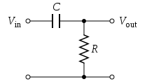 The simple first-order electronic high-pass filter shown in Figure 1 is implemented by placing an input voltage across the series combination of a capacitor and a resistor and using the voltage across the resistor as an output. The product of the resistance and capacitance (R×C) is the time constant (τ); it is inversely proportional to the cutoff frequency fc, that is,
Figure 2 shows an active electronic implementation of a first-order high-pass filter using an operational amplifier. In this case, the filter has a passband gain of -R2/R1 and has a cutoff frequency of
From the circuit in Figure 1 above, according to Kirchhoff's Laws and the definition of capacitance:
First-order continuous-time implementation

Figure 1: A passive, analog, first-order high-pass filter, realized by an RC circuit

Figure 2 shows an active electronic implementation of a first-order high-pass filter using an operational amplifier. In this case, the filter has a passband gain of -R2/R1 and has a cutoff frequency of


Discrete-time realization
Discrete-time high-pass filters can also be designed. Discrete-time filter design is beyond the scope of this article; however, a simple example comes from the conversion of the continuous-time high-pass filter above to a discrete-time realization. That is, the continuous-time behavior can be discretized.From the circuit in Figure 1 above, according to Kirchhoff's Laws and the definition of capacitance:


- .

- so


- .


Algorithmic implementation
The filter recurrence relation provides a way to determine the output samples in terms of the input samples and the preceding output. The following pseudocode algorithm will simulate the effect of a high-pass filter on a series of digital samples:Sunday, 24 September 2017
A low-pass filter
A low-pass filter (LPF) is a filter that passes signals with a frequency lower than a certain cutoff frequency and attenuates signals with frequencies higher than the cutoff frequency. The exact frequency response of the filter depends on the filter design. The filter is sometimes called a high-cut filter, or treble-cut filter in audio applications. A low-pass filter is the complement of a high-pass filter.
Low-pass filters exist in many different forms, including electronic circuits such as a hiss filter used in audio, anti-aliasing filters for conditioning signals prior to analog-to-digital conversion, digital filters for smoothing sets of data, acoustic barriers, blurring of images, and so on. The moving average operation used in fields such as finance is a particular kind of low-pass filter, and can be analyzed with the same signal processing techniques as are used for other low-pass filters. Low-pass filters provide a smoother form of a signal, removing the short-term fluctuations, and leaving the longer-term trend.
Filter designers will often use the low-pass form as a prototype filter. That is, a filter with unity bandwidth and impedance. The desired filter is obtained from the prototype by scaling for the desired bandwidth and impedance and transforming into the desired bandform (that is low-pass, high-pass, band-pass or band-stop).
Electronic low-pass filters are used on inputs to subwoofers and other types of loudspeakers, to block high pitches that they can't efficiently reproduce. Radio transmitters use low-pass filters to block harmonic emissions that might interfere with other communications. The tone knob on many electric guitars is a low-pass filter used to reduce the amount of treble in the sound. An integrator is another time constant low-pass filter.
Telephone lines fitted with DSL splitters use low-pass and high-pass filters to separate DSL and POTS signals sharing the same pair of wires.
Low-pass filters also play a significant role in the sculpting of sound created by analogue and virtual analogue synthesisers. See subtractive synthesis.
Low-pass filters exist in many different forms, including electronic circuits such as a hiss filter used in audio, anti-aliasing filters for conditioning signals prior to analog-to-digital conversion, digital filters for smoothing sets of data, acoustic barriers, blurring of images, and so on. The moving average operation used in fields such as finance is a particular kind of low-pass filter, and can be analyzed with the same signal processing techniques as are used for other low-pass filters. Low-pass filters provide a smoother form of a signal, removing the short-term fluctuations, and leaving the longer-term trend.
Filter designers will often use the low-pass form as a prototype filter. That is, a filter with unity bandwidth and impedance. The desired filter is obtained from the prototype by scaling for the desired bandwidth and impedance and transforming into the desired bandform (that is low-pass, high-pass, band-pass or band-stop).
Examples
Examples of low-pass filters occur in acoustics, optics and electronics.Acoustics
A stiff physical barrier tends to reflect higher sound frequencies, and so acts as a low-pass filter for transmitting sound. When music is playing in another room, the low notes are easily heard, while the high notes are attenuated.Optics
An optical filter with the same function can correctly be called a low-pass filter, but conventionally is called a longpass filter (low frequency is long wavelength), to avoid confusion.Electronics
In an electronic low-pass RC filter for voltage signals, high frequencies in the input signal are attenuated, but the filter has little attenuation below the cutoff frequency determined by its RC time constant. For current signals, a similar circuit, using a resistor and capacitor in parallel, works in a similar manner. (See current divider discussed in more detail below.)Electronic low-pass filters are used on inputs to subwoofers and other types of loudspeakers, to block high pitches that they can't efficiently reproduce. Radio transmitters use low-pass filters to block harmonic emissions that might interfere with other communications. The tone knob on many electric guitars is a low-pass filter used to reduce the amount of treble in the sound. An integrator is another time constant low-pass filter.
Telephone lines fitted with DSL splitters use low-pass and high-pass filters to separate DSL and POTS signals sharing the same pair of wires.
Low-pass filters also play a significant role in the sculpting of sound created by analogue and virtual analogue synthesisers. See subtractive synthesis.
Saturday, 23 September 2017
Electronic filter
Electronic filters are circuits which perform signal processing functions, specifically to remove unwanted frequency components from the signal, to enhance wanted ones, or both. Electronic filters can be:
Hybrid filters are also possible, typically involving a combination of analog amplifiers with mechanical resonators or delay lines. Other devices such as CCD delay lines have also been used as discrete-time filters. With the availability of digital signal processing, active digital filters have become common.
Inductors block high-frequency signals and conduct low-frequency signals, while capacitors do the reverse. A filter in which the signal passes through an inductor, or in which a capacitor provides a path to ground, presents less attenuation to low-frequency signals than high-frequency signals and is therefore a low-pass filter. If the signal passes through a capacitor, or has a path to ground through an inductor, then the filter presents less attenuation to high-frequency signals than low-frequency signals and therefore is a high-pass filter. Resistors on their own have no frequency-selective properties, but are added to inductors and capacitors to determine the time-constants of the circuit, and therefore the frequencies to which it responds.
The inductors and capacitors are the reactive elements of the filter. The number of elements determines the order of the filter. In this context, an LC tuned circuit being used in a band-pass or band-stop filter is considered a single element even though it consists of two components.
At high frequencies (above about 100 megahertz), sometimes the inductors consist of single loops or strips of sheet metal, and the capacitors consist of adjacent strips of metal. These inductive or capacitive pieces of metal are called stubs.
- passive or active
- analog or digital
- high-pass, low-pass, band-pass, band-stop (band-rejection; notch), or all-pass.
- discrete-time (sampled) or continuous-time
- linear or non-linear
- infinite impulse response (IIR type) or finite impulse response (FIR type)
History
The oldest forms of electronic filters are passive analog linear filters, constructed using only resistors and capacitors or resistors and inductors. These are known as RC and RL single-pole filters respectively. More complex multipole LC filters have also existed for many years, and their operation is well understood.Hybrid filters are also possible, typically involving a combination of analog amplifiers with mechanical resonators or delay lines. Other devices such as CCD delay lines have also been used as discrete-time filters. With the availability of digital signal processing, active digital filters have become common.
Classification by technology
Passive filters
Passive implementations of linear filters are based on combinations of resistors (R), inductors (L) and capacitors (C). These types are collectively known as passive filters, because they do not depend upon an external power supply and/or they do not contain active components such as transistors.Inductors block high-frequency signals and conduct low-frequency signals, while capacitors do the reverse. A filter in which the signal passes through an inductor, or in which a capacitor provides a path to ground, presents less attenuation to low-frequency signals than high-frequency signals and is therefore a low-pass filter. If the signal passes through a capacitor, or has a path to ground through an inductor, then the filter presents less attenuation to high-frequency signals than low-frequency signals and therefore is a high-pass filter. Resistors on their own have no frequency-selective properties, but are added to inductors and capacitors to determine the time-constants of the circuit, and therefore the frequencies to which it responds.
The inductors and capacitors are the reactive elements of the filter. The number of elements determines the order of the filter. In this context, an LC tuned circuit being used in a band-pass or band-stop filter is considered a single element even though it consists of two components.
At high frequencies (above about 100 megahertz), sometimes the inductors consist of single loops or strips of sheet metal, and the capacitors consist of adjacent strips of metal. These inductive or capacitive pieces of metal are called stubs.
Friday, 22 September 2017
Crossed-field amplifier
A crossed-field amplifier (CFA) is a specialized vacuum tube, first introduced in the mid-1950s and frequently used as a microwave amplifier in very-high-power transmitters.
Raytheon engineer William C. Brown's work to adapt magnetron principles to create a new broadband amplifier is generally recognized as the first CFA, which he called an Amplitron. Other names that are sometimes used by CFA manufacturers include Platinotron or Stabilotron.
A CFA has lower gain and bandwidth than other microwave amplifier tubes (such as klystrons or traveling-wave tubes); but it is more efficient and capable of much higher output power.
Peak output powers of many megawatts and average power levels of tens of kilowatts can be achieved, with efficiency ratings in excess of 70 percent. Their current use is in ground stations for TVRO broadcasting and Deep Space telecommunications networks.
The CFA has the useful property that when power is shut off, the input simply passes to the output with very little loss. This avoids the need for RF bypass switching in the event of failure.
Two CFAs can be connected sequentially with only one powered; if it fails, power can be removed from the primary tube and applied to the secondary as a backup. This approach with built-in redundancy was used on the S-band downlink transmitter on the Apollo Lunar Module where high efficiency and reliability were needed.
A large negative voltage is placed on the green electrode in the center, and a large magnetic field is directed perpendicular to the page. This forms a thin spinning disk of electrons with a flow pattern like spinning water as it drains from a sink or toilet. A slow-wave structure is located above and below the spinning disk of electrons. Electrons flow much slower than the speed of light, and the slow wave structure reduces the velocity of the input RF enough to match the electron velocity.
The RF input is introduced into the slow wave structure. The alternating microwave field causes the electrons to alternately speed up and slow down. These disturbances grow larger as electrons spiral around the device, and electrons slow down as the RF energy grows. This produces amplification.
There is a small amount of RF feedback from output to input. This creates a slight random phase jitter when the device is pulsed.
Raytheon engineer William C. Brown's work to adapt magnetron principles to create a new broadband amplifier is generally recognized as the first CFA, which he called an Amplitron. Other names that are sometimes used by CFA manufacturers include Platinotron or Stabilotron.
A CFA has lower gain and bandwidth than other microwave amplifier tubes (such as klystrons or traveling-wave tubes); but it is more efficient and capable of much higher output power.
Peak output powers of many megawatts and average power levels of tens of kilowatts can be achieved, with efficiency ratings in excess of 70 percent. Their current use is in ground stations for TVRO broadcasting and Deep Space telecommunications networks.
Operation
The electric and magnetic fields in a CFA are perpendicular to each other ("crossed fields"). This is the same type of field interaction used in a magnetron; as a result, the two devices share many characteristics (such as high peak power and efficiency) and they have similar physical appearances. However, a magnetron is an oscillator and a CFA is an amplifier (although a CFA can be driven to oscillate by application of improper low voltages as can any amplifier); a CFA's RF circuit (or slow-wave structure) is similar to that in a coupled-cavity TWT.The CFA has the useful property that when power is shut off, the input simply passes to the output with very little loss. This avoids the need for RF bypass switching in the event of failure.
Two CFAs can be connected sequentially with only one powered; if it fails, power can be removed from the primary tube and applied to the secondary as a backup. This approach with built-in redundancy was used on the S-band downlink transmitter on the Apollo Lunar Module where high efficiency and reliability were needed.
A large negative voltage is placed on the green electrode in the center, and a large magnetic field is directed perpendicular to the page. This forms a thin spinning disk of electrons with a flow pattern like spinning water as it drains from a sink or toilet. A slow-wave structure is located above and below the spinning disk of electrons. Electrons flow much slower than the speed of light, and the slow wave structure reduces the velocity of the input RF enough to match the electron velocity.
The RF input is introduced into the slow wave structure. The alternating microwave field causes the electrons to alternately speed up and slow down. These disturbances grow larger as electrons spiral around the device, and electrons slow down as the RF energy grows. This produces amplification.
There is a small amount of RF feedback from output to input. This creates a slight random phase jitter when the device is pulsed.
Thursday, 21 September 2017
Voltage-regulator tube
A voltage-regulator tube (VR tube) is an electronic component used as a shunt regulator to hold a voltage constant at a pre-determined level.
Physically, these devices resemble vacuum tubes, but there are two main differences:
Because the device would conduct a nearly unlimited amount of current, there must be some external means of limiting the current. Usually, this is provided by an external resistor upstream from the VR tube. The VR tube then conducts any portion of the current that does not flow into the downstream load, maintaining an approximately constant voltage across the VR tube's electrodes. The VR tube's regulation voltage was only guaranteed when conducting an amount of current within the allowable range. In particular, if the current through the tube is too low to maintain ionization, the output voltage can rise above the nominal output—as far as the input supply voltage. If the current through the tube is too high, it can enter an arc discharge mode where the voltage will be significantly lower than nominal and the tube may be damaged.
Some voltage-regulator tubes contained small amounts of radionuclides to produce a more reliable ionization.
The Corona VR tube is a high-voltage version that's hydrogen-filled at close to atmospheric pressure, for voltages ranging from 400 V to 30 kV at tens of microamperes. It has a coaxial form; the outer cylindrical electrode is the cathode and the inner one is the anode. The voltage stability depends on the gas pressure.
Physically, these devices resemble vacuum tubes, but there are two main differences:
- Their glass envelopes are filled with a gas mixture, and
- They have a cold cathode; the cathode is not heated with a filament to emit electrons.
- They rely on gas ionization, rather than Zener breakdown
- The unregulated supply voltage must be 15–20% above the nominal output voltage to ensure that the discharge starts
- The output can be higher than nominal if the current through the tube is too low.
Because the device would conduct a nearly unlimited amount of current, there must be some external means of limiting the current. Usually, this is provided by an external resistor upstream from the VR tube. The VR tube then conducts any portion of the current that does not flow into the downstream load, maintaining an approximately constant voltage across the VR tube's electrodes. The VR tube's regulation voltage was only guaranteed when conducting an amount of current within the allowable range. In particular, if the current through the tube is too low to maintain ionization, the output voltage can rise above the nominal output—as far as the input supply voltage. If the current through the tube is too high, it can enter an arc discharge mode where the voltage will be significantly lower than nominal and the tube may be damaged.
Some voltage-regulator tubes contained small amounts of radionuclides to produce a more reliable ionization.
The Corona VR tube is a high-voltage version that's hydrogen-filled at close to atmospheric pressure, for voltages ranging from 400 V to 30 kV at tens of microamperes. It has a coaxial form; the outer cylindrical electrode is the cathode and the inner one is the anode. The voltage stability depends on the gas pressure.
Wednesday, 20 September 2017
Force-sensing resistor
A force-sensing resistor is a material whose resistance changes when a force or pressure is applied. They are also known as "force-sensitive resistor" and are sometimes referred to by the initialism "FSR".
History
The technology of force-sensing resistors was invented and patented in 1977 by Franklin Eventoff. In 1985 Eventoff founded Interlink Electronics, a company based on his force-sensing-resistor (FSR). In 1987, Eventoff was the recipient of the prestigious international IR 100 award for the development of the FSR. In 2001 Eventoff founded a new company, Sensitronics,which has become the leader in developing force-sensing resistor technology worldwide.Properties
Force-sensing resistors consist of a conductive polymer, which changes resistance in a predictable manner following application of force to its surface.They are normally supplied as a polymer sheet or ink that can be applied by screen printing. The sensing film consists of both electrically conducting and non-conducting particles suspended in matrix. The particles are sub-micrometre sizes, and are formulated to reduce the temperature dependence, improve mechanical properties and increase surface durability. Applying a force to the surface of the sensing film causes particles to touch the conducting electrodes, changing the resistance of the film. As with all resistive based sensors, force-sensing resistors require a relatively simple interface and can operate satisfactorily in moderately hostile environments. Compared to other force sensors, the advantages of FSRs are their size (thickness typically less than 0.5 mm), low cost and good shock resistance. A disadvantage is their low precision: measurement results may differ 10% and more.Uses
Force-sensing resistors are commonly used to create pressure-sensing "buttons" and have applications in many fields, including musical instruments, car occupancy sensors, artificial limbs, Foot pronation systems and portable electronics.Tuesday, 19 September 2017
Returning to normal posts
Hi folks I soon will be returning to the normal post starting with Circuit Monday on 2nd of October I am hoping that this will be the last break from the schedule I will have to take for a while. thank you for continuing to read the post .
all the best dobby
all the best dobby
Monday, 18 September 2017
PCF8591P
Philips Semiconductors Product specification
8-bit A/D and D/A converter PCF8591
1 FEATURES
• Single power supply • Operating supply voltage 2.5 V to 6 V • Low standby current • Serial input/output via I2C-bus • Address by 3 hardware address pins • Sampling rate given by I2C-bus speed • 4 analog inputs programmable as single-ended or differential inputs
• Auto-incremented channel selection • Analog voltage range from VSS to VDD • On-chip track and hold circuit • 8-bit successive approximation A/D conversion • Multiplying DAC with one analog output.
2 APPLICATIONS
• Closed loop control systems • Low power converter for remote data acquisition • Battery operated equipment • Acquisition of analog values in automotive, audio and TV applications.
3 GENERAL DESCRIPTION
The PCF8591 is a single-chip, single-supply low power 8-bit CMOS data acquisition device with four analog inputs, one analog output and a serial I2C-bus interface. Three address pins A0, A1 and A2 are used for programming the hardware address, allowing the use of up to eight devices connected to the I2C-bus without additional hardware. Address, control and data to and from the device are transferred serially via the two-line bidirectional I2C-bus.
The functions of the device include analog input multiplexing, on-chip track and hold function, 8-bit analog-to-digital conversion and an 8-bit digital-to-analog conversion. The maximum conversion rate is given by the maximum speed of the I2C-bus.
4 ORDERING INFORMATION
TYPE NUMBER
PACKAGE
NAME DESCRIPTION VERSION
PCA8591P DIP16 plastic dual in-line package; 16 leads (300 mil); long body SOT38-1 PCA8591T SO16 plastic small outline package; 16 leads; body width 7.5 mm SOT162-1
1998 Jul 02 4
Philips Semiconductors Product specification
8-bit A/D and D/A converter PCF8591
This text is here in white to force landscape pages to be rotated correctly when browsing through the pdf in the Acrobat reader.This text is here in _white to force landscape pages to be rotated correctly when browsing through the pdf in the Acrobat reader.This text is here inThis text is here in white to force landscape pages to be rotated correctly when browsing through the pdf in the Acrobat reader. white to force landscape pages to be ...
5 BLOCK DIAGRAM
Fig.1 Block diagram.
1998 Jul 02 5
Philips Semiconductors Product specification
8-bit A/D and D/A converter PCF8591
6 PINNING
SYMBOL PIN DESCRIPTION
AINO 1
analog inputs (A/D converter)
AIN1 2 AIN2 3 AIN3 4 A0 5 hardware addressA1 6 A2 7 VSS 8 negative supply voltage SDA 9 I2C-bus data input/output SCL 10 I2C-bus clock input OSC 11 oscillator input/output EXT 12 external/internal switch for oscillator input AGND 13 analog ground VREF 14 voltage reference input AOUT 15 analog output (D/A converter) VDD 16 positive supply voltage
Fig.2 Pinning diagram.
8-bit A/D and D/A converter PCF8591
1 FEATURES
• Single power supply • Operating supply voltage 2.5 V to 6 V • Low standby current • Serial input/output via I2C-bus • Address by 3 hardware address pins • Sampling rate given by I2C-bus speed • 4 analog inputs programmable as single-ended or differential inputs
• Auto-incremented channel selection • Analog voltage range from VSS to VDD • On-chip track and hold circuit • 8-bit successive approximation A/D conversion • Multiplying DAC with one analog output.
2 APPLICATIONS
• Closed loop control systems • Low power converter for remote data acquisition • Battery operated equipment • Acquisition of analog values in automotive, audio and TV applications.
3 GENERAL DESCRIPTION
The PCF8591 is a single-chip, single-supply low power 8-bit CMOS data acquisition device with four analog inputs, one analog output and a serial I2C-bus interface. Three address pins A0, A1 and A2 are used for programming the hardware address, allowing the use of up to eight devices connected to the I2C-bus without additional hardware. Address, control and data to and from the device are transferred serially via the two-line bidirectional I2C-bus.
The functions of the device include analog input multiplexing, on-chip track and hold function, 8-bit analog-to-digital conversion and an 8-bit digital-to-analog conversion. The maximum conversion rate is given by the maximum speed of the I2C-bus.
4 ORDERING INFORMATION
TYPE NUMBER
PACKAGE
NAME DESCRIPTION VERSION
PCA8591P DIP16 plastic dual in-line package; 16 leads (300 mil); long body SOT38-1 PCA8591T SO16 plastic small outline package; 16 leads; body width 7.5 mm SOT162-1
1998 Jul 02 4
Philips Semiconductors Product specification
8-bit A/D and D/A converter PCF8591
This text is here in white to force landscape pages to be rotated correctly when browsing through the pdf in the Acrobat reader.This text is here in _white to force landscape pages to be rotated correctly when browsing through the pdf in the Acrobat reader.This text is here inThis text is here in white to force landscape pages to be rotated correctly when browsing through the pdf in the Acrobat reader. white to force landscape pages to be ...
5 BLOCK DIAGRAM
Fig.1 Block diagram.
1998 Jul 02 5
Philips Semiconductors Product specification
8-bit A/D and D/A converter PCF8591
6 PINNING
SYMBOL PIN DESCRIPTION
AINO 1
analog inputs (A/D converter)
AIN1 2 AIN2 3 AIN3 4 A0 5 hardware addressA1 6 A2 7 VSS 8 negative supply voltage SDA 9 I2C-bus data input/output SCL 10 I2C-bus clock input OSC 11 oscillator input/output EXT 12 external/internal switch for oscillator input AGND 13 analog ground VREF 14 voltage reference input AOUT 15 analog output (D/A converter) VDD 16 positive supply voltage
Fig.2 Pinning diagram.
Sunday, 17 September 2017
Multiplexer
In electronics, a multiplexer (or mux) is a device that selects one of several analog or digital input signals and forwards the selected input into a single line.A multiplexer of 2n inputs has ⌈n⌉ select lines, which are used to select which input line to send to the output.Multiplexers are mainly used to increase the amount of data that can be sent over the network within a certain amount of time and bandwidth. A multiplexer is also called a data selector. Multiplexers can also be used to implement Boolean functions of multiple variables.
An electronic multiplexer makes it possible for several signals to share one device or resource, for example, one A/D converter or one communication line, instead of having one device per input signal.
Conversely, a demultiplexer (or demux) is a device taking a single input signal and selecting one of many data-output-lines, which is connected to the single input. A multiplexer is often used with a complementary demultiplexer on the receiving end.
An electronic multiplexer can be considered as a multiple-input, single-output switch, and a demultiplexer as a single-input, multiple-output switch. The schematic symbol for a multiplexer is an isosceles trapezoid with the longer parallel side containing the input pins and the short parallel side containing the output pin. The schematic on the right shows a 2-to-1 multiplexer on the left and an equivalent switch on the right. The wire connects the desired input to the output.
For example, 9 to 16 inputs would require no fewer than 4 selector pins and 17 to 32 inputs would require no fewer than 5 selector pins. The binary value expressed on these selector pins determines the selected input pin.
If X is the input and S is the selector, and A and B are the outputs:
An electronic multiplexer makes it possible for several signals to share one device or resource, for example, one A/D converter or one communication line, instead of having one device per input signal.
Conversely, a demultiplexer (or demux) is a device taking a single input signal and selecting one of many data-output-lines, which is connected to the single input. A multiplexer is often used with a complementary demultiplexer on the receiving end.
An electronic multiplexer can be considered as a multiple-input, single-output switch, and a demultiplexer as a single-input, multiple-output switch. The schematic symbol for a multiplexer is an isosceles trapezoid with the longer parallel side containing the input pins and the short parallel side containing the output pin. The schematic on the right shows a 2-to-1 multiplexer on the left and an equivalent switch on the right. The wire connects the desired input to the output.

Digital multiplexers
In digital circuit design, the selector wires are of digital value. In the case of a 2-to-1 multiplexer, a logic value of 0 would connect to the output while a logic value of 1 would connect to the output. In larger multiplexers, the number of selector pins is equal to where is the number of inputs.


For example, 9 to 16 inputs would require no fewer than 4 selector pins and 17 to 32 inputs would require no fewer than 5 selector pins. The binary value expressed on these selector pins determines the selected input pin.
Chaining multiplexers
Larger Multiplexers can be constructed by using smaller multiplexers by chaining them together. For example, an 8-to-1 multiplexer can be made with two 4-to-1 and one 2-to-1 multiplexers. The two 4-to-1 multiplexer outputs are fed into the 2-to-1 with the selector pins on the 4-to-1's put in parallel giving a total number of selector inputs to 3, which is equivalent to an 8-to-1.Digital demultiplexers
Demultiplexers take one data input and a number of selection inputs, and they have several outputs. They forward the data input to one of the outputs depending on the values of the selection inputs. Demultiplexers are sometimes convenient for designing general purpose logic, because if the demultiplexer's input is always true, the demultiplexer acts as a decoder. This means that any function of the selection bits can be constructed by logically OR-ing the correct set of outputs.If X is the input and S is the selector, and A and B are the outputs:


.jpg)
Saturday, 16 September 2017
Counter
A counter circuit is usually constructed of a number of flip-flops connected in cascade. Counters are a very widely used component in digital circuits, and are manufactured as separate integrated circuits and also incorporated as parts of larger integrated circuits.
Occasionally there are advantages to using a counting sequence other than the natural binary sequence—such as the binary coded decimal counter, a linear-feedback shift register counter, or a Gray-code counter.
Counters are useful for digital clocks and timers, and in oven timers, VCR clocks, etc.
Electronic counters
In electronics, counters can be implemented quite easily using register-type circuits such as the flip-flop, and a wide variety of classifications exist:- Asynchronous (ripple) counter – changing state bits are used as clocks to subsequent state flip-flops
- Synchronous counter – all state bits change under control of a single clock
- Decade counter – counts through ten states per stage
- Up/down counter – counts both up and down, under command of a control input
- Ring counter – formed by a shift register with feedback connection in a ring
- Johnson counter – a twisted ring counter
- Cascaded counter
- Modulus counter.
Occasionally there are advantages to using a counting sequence other than the natural binary sequence—such as the binary coded decimal counter, a linear-feedback shift register counter, or a Gray-code counter.
Counters are useful for digital clocks and timers, and in oven timers, VCR clocks, etc.
Friday, 15 September 2017
Adder
An adder is a digital circuit that performs addition of numbers. In many computers and other kinds of processors adders are used in the arithmetic logic units. They are also utilized in other parts of the processor, where they are used to calculate addresses, table indices, increment and decrement operators, and similar operations.
Although adders can be constructed for many number representations, such as binary-coded decimal or excess-3, the most common adders operate on binary numbers. In cases where two's complement or ones' complement is being used to represent negative numbers, it is trivial to modify an adder into an adder–subtractor. Other signed number representations require more logic around the basic adder.
The half adder adds two single binary digits A and B. It has two outputs, sum (S) and carry (C). The carry signal represents an overflow into the next digit of a multi-digit addition. The value of the sum in decimal system is 2C + S. The simplest half-adder design, pictured on the right, incorporates an XOR gate for S and an AND gate for C. The Boolean logic for the sum (in this case S) will be A'B+AB' whereas for carry (C) will be AB. With the addition of an OR gate to combine their carry outputs, two half adders can be combined to make a full adder. The half adder adds two input bits and generates a carry and sum, which are the two outputs of a half adder. The input variables of a half adder are called the augend and addend bits. The output variables are the sum and carry.
Thursday, 14 September 2017
Flip-flop
In electronics, a flip-flop or latch is a circuit that has two stable states and can be used to store state information. A flip-flop is a bistable multivibrator. The circuit can be made to change state by signals applied to one or more control inputs and will have one or two outputs. It is the basic storage element in sequential logic. Flip-flops and latches are fundamental building blocks of digital electronics systems used in computers, communications, and many other types of systems.
Flip-flops and latches are used as data storage elements. A flip-flop stores a single bit (binary digit) of data; one of its two states represents a "one" and the other represents a "zero". Such data storage can be used for storage of state, and such a circuit is described as sequential logic. When used in a finite-state machine, the output and next state depend not only on its current input, but also on its current state (and hence, previous inputs). It can also be used for counting of pulses, and for synchronizing variably-timed input signals to some reference timing signal.
Flip-flops can be either simple (transparent or opaque) or clocked (synchronous or edge-triggered). Although the term flip-flop has historically referred generically to both simple and clocked circuits, in modern usage it is common to reserve the term flip-flop exclusively for discussing clocked circuits; the simple ones are commonly called latches.
Using this terminology, a latch is level-sensitive, whereas a flip-flop is edge-sensitive. That is, when a latch is enabled it becomes transparent, while a flip flop's output only changes on a single type (positive going or negative going) of clock edge
According to P. L. Lindley, an engineer at the US Jet Propulsion Laboratory, the flip-flop types detailed below (SR, D, T, JK) were first discussed in a 1954 UCLA course on computer design by Montgomery Phister, and then appeared in his book Logical Design of Digital Computers.Lindley was at the time working at Hughes Aircraft under Eldred Nelson, who had coined the term JK for a flip-flop which changed states when both inputs were on (a logical "one"). The other names were coined by Phister. They differ slightly from some of the definitions given below. Lindley explains that he heard the story of the JK flip-flop from Eldred Nelson, who is responsible for coining the term while working at Hughes Aircraft. Flip-flops in use at Hughes at the time were all of the type that came to be known as J-K. In designing a logical system, Nelson assigned letters to flip-flop inputs as follows: #1: A & B, #2: C & D, #3: E & F, #4: G & H, #5: J & K. Nelson used the notations "j-input" and "k-input" in a patent application filed in 1953.
Simple flip-flops can be built around a single pair of cross-coupled inverting elements: vacuum tubes, bipolar transistors, field effect transistors, inverters, and inverting logic gates have all been used in practical circuits.
Clocked devices are specially designed for synchronous systems; such devices ignore their inputs except at the transition of a dedicated clock signal (known as clocking, pulsing, or strobing). Clocking causes the flip-flop either to change or to retain its output signal based upon the values of the input signals at the transition. Some flip-flops change output on the rising edge of the clock, others on the falling edge.
Since the elementary amplifying stages are inverting, two stages can be connected in succession (as a cascade) to form the needed non-inverting amplifier. In this configuration, each amplifier may be considered as an active inverting feedback network for the other inverting amplifier. Thus the two stages are connected in a non-inverting loop although the circuit diagram is usually drawn as a symmetric cross-coupled pair
Flip-flops and latches are used as data storage elements. A flip-flop stores a single bit (binary digit) of data; one of its two states represents a "one" and the other represents a "zero". Such data storage can be used for storage of state, and such a circuit is described as sequential logic. When used in a finite-state machine, the output and next state depend not only on its current input, but also on its current state (and hence, previous inputs). It can also be used for counting of pulses, and for synchronizing variably-timed input signals to some reference timing signal.
Flip-flops can be either simple (transparent or opaque) or clocked (synchronous or edge-triggered). Although the term flip-flop has historically referred generically to both simple and clocked circuits, in modern usage it is common to reserve the term flip-flop exclusively for discussing clocked circuits; the simple ones are commonly called latches.
Using this terminology, a latch is level-sensitive, whereas a flip-flop is edge-sensitive. That is, when a latch is enabled it becomes transparent, while a flip flop's output only changes on a single type (positive going or negative going) of clock edge
History
The first electronic flip-flop was invented in 1918 by the British physicists William Eccles and F. W. Jordan.It was initially called the Eccles–Jordan trigger circuit and consisted of two active elements (vacuum tubes). The design was used in the 1943 British Colossus codebreaking computer and such circuits and their transistorized versions were common in computers even after the introduction of integrated circuits, though flip-flops made from logic gates are also common now. Early flip-flops were known variously as trigger circuits or multivibrators.According to P. L. Lindley, an engineer at the US Jet Propulsion Laboratory, the flip-flop types detailed below (SR, D, T, JK) were first discussed in a 1954 UCLA course on computer design by Montgomery Phister, and then appeared in his book Logical Design of Digital Computers.Lindley was at the time working at Hughes Aircraft under Eldred Nelson, who had coined the term JK for a flip-flop which changed states when both inputs were on (a logical "one"). The other names were coined by Phister. They differ slightly from some of the definitions given below. Lindley explains that he heard the story of the JK flip-flop from Eldred Nelson, who is responsible for coining the term while working at Hughes Aircraft. Flip-flops in use at Hughes at the time were all of the type that came to be known as J-K. In designing a logical system, Nelson assigned letters to flip-flop inputs as follows: #1: A & B, #2: C & D, #3: E & F, #4: G & H, #5: J & K. Nelson used the notations "j-input" and "k-input" in a patent application filed in 1953.
Implementation
Flip-flops can be either simple (transparent or asynchronous) or clocked (synchronous). The simple ones are commonly described as latches, while the clocked ones are described as flip-flopsSimple flip-flops can be built around a single pair of cross-coupled inverting elements: vacuum tubes, bipolar transistors, field effect transistors, inverters, and inverting logic gates have all been used in practical circuits.
Clocked devices are specially designed for synchronous systems; such devices ignore their inputs except at the transition of a dedicated clock signal (known as clocking, pulsing, or strobing). Clocking causes the flip-flop either to change or to retain its output signal based upon the values of the input signals at the transition. Some flip-flops change output on the rising edge of the clock, others on the falling edge.
Since the elementary amplifying stages are inverting, two stages can be connected in succession (as a cascade) to form the needed non-inverting amplifier. In this configuration, each amplifier may be considered as an active inverting feedback network for the other inverting amplifier. Thus the two stages are connected in a non-inverting loop although the circuit diagram is usually drawn as a symmetric cross-coupled pair
Subscribe to:
Posts (Atom)
-
a vacuum tube , an electron tube ,or just a tube (North America), or valve (Britain and some other regions), is a device that controls ele...
-
 welcome and happy Project day this week it is a Prototyping board for bread boarding this was just a quick little project to give me an eas...
 -
hi guys I just wanted to share this Electrical Contact Cleaner I got from ebay to it works really well and does the job